


Germanium photodiodes are widely used for measuring optical power in the near-infrared (NIR) range, particularly in cost-sensitive systems or applications requiring large-area detectors. Compared with similarly sized InGaAs detectors, however, germanium devices typically exhibit lower shunt resistance and higher dark current, which leads to increased noise.
As a result, germanium photodiodes are best suited for applications in which the detected signal is significantly higher than the noise floor. To improve performance, GPD Optoelectronics offers its “HS” series of germanium photodiodes, designed with higher-than-typical shunt resistance.
-
Features
- Chip diameters from 1 mm to 25 mm
- Spectral response from 800 nm to 1700 nm
- High linearity > 10 dBm
- Multiple window and lens options
- Optical filters available (neutral density, bandpass, etc.)
- Thermoelectric cooling options
- Wide packaging variety: TO packages, BNC options, chip on ceramic submount, and more
-
Applications
- Optical power meters
- LED/LD characterization and burn-in diagnostics
- Spectroscopy
- Eye-safe laser detection sensors
-
Operating Voltage
We offer several germanium chip designs based on the preferred operating voltage.
- GM series: Designed for high-speed applications with reverse bias > 10 V
- HS series: Designed for applications with reverse bias < 5 V
- VHS series: Designed for zero-bias applications
- VHR series: Designed for zero-bias applications requiring high shunt resistance
-
Packaging Capablilities
| Packaging Configurations | ||||||||
| Size | TO Headers | Ceramic Leadless Chip Carriers |
||||||
| TO-46 | TO-18 | TO-5 | TO-8 | TO-9 | LCC-6 | LCC-28 | BNC | |
| 1 mm dia. | ● | ● | ● | |||||
| 2 mm dia. | ● | ● | ||||||
| 3 mm dia. | ● | ● | ● | |||||
| 5 mm dia. | ● | ● | ● | |||||
| 10x10 mm | ● | ● | ||||||
| Window (Other Options Available) | ||||||||
| Material | Molded Clear Glass | Sapphire | Borosilicate Glass | |||||
| Thickness (mm) | 0.25 | 0.5 | 0.5 | |||||
-
Specifications
1 mm Diameter Germanium Photodiode Performance Specifications
| Part Number | GB100-XX | GH100-XX | GV100-XX | |
| Optoelectronic Characteristics @ 23 ºC ± 2 ºC | Units | |||
| RSHUNT @ 10mV (min/typ) | 20/40 | 60/100 | 200/280 | kΩ |
| IDARK (max) | 4 | 1.5 | 0.5 | μA |
| Capacitance (max) | 95 | 300 | 1500 | pF |
| VREVERSE | 15 | 2 | 0.3 | V |
| NEP (typ) | 1.5 | 1 | 0.6 | pW/Hz1/2 |
| Maximum Reverse Voltage | 15 | 3 | 0.3 | V |
2 mm Diameter Germanium Photodiode Performance Specifications
| Part Number | GB200-XX | GH200-XX | GV200-XX | |
| Optoelectronic Characteristics @ 23 ºC ± 2 ºC | Units | |||
| RSHUNT @ 10mV (min/typ) | 6/12 | 30/60 | 80/120 | kΩ |
| IDARK (max) | 10 | 3 | 1 | μA |
| Capacitance (max) | 360 | 2200 | 7000 | pF |
| VREVERSE | 10 | 2 | 0.3 | V |
| NEP (typ) | 3 | 1.4 | 0.8 | pW/Hz1/2 |
| Maximum Reverse Voltage | 15 | 3 | 0.5 | V |
3 mm Diameter Germanium Photodiode Performance Specifications
| Part Number | GB300-XX | GH300-XX | GV300-XX | |
| Optoelectronic Characteristics @ 23 ºC ± 2 ºC | Units | |||
| RSHUNT @ 10mV (min/typ) | 4/8 | 25/35 | 40/65 | kΩ |
| IDARK (max) | 20 | 4 | 2 | μA |
| Capacitance (max) | 1200 | 7000 | 14000 | pF |
| VREVERSE | 5 | 1 | 0.25 | V |
| NEP (typ) | 4 | 2 | 1 | pW/Hz1/2 |
| Maximum Reverse Voltage | 10 | 3 | 0.5 | V |
5 mm Diameter Germanium Photodiode Performance Specifications
| Part Number | GB500-XX | GH500-XX | GV500-XX | |
| Optoelectronic Characteristics @ 23 ºC ± 2 ºC | Units | |||
| RSHUNT @ 10mV (min/typ) | 2/4 | 10/15 | 15/20 | kΩ |
| IDARK (max) | 30 | 10 | 5 | μA |
| Capacitance (max) | 3000 | 17000 | 40000 | pF |
| VREVERSE | 3 | 1 | 0.1 | V |
| NEP (typ) | 5 | 3 | 2 | pW/Hz1/2 |
| Maximum Reverse Voltage | 10 | 3 | 0.3 | V |
10 x 10 mm Diameter Germanium Photodiode Performance Specifications
| Part Number | GB10M-XX | GH10M-XX | GV10M-XX | |
| Optoelectronic Characteristics @ 23 ºC ± 2 ºC | Units | |||
| RSHUNT @ 10mV (min/typ) | Contact us for more information |
2/3.5 | Contact us for more information |
kΩ |
| IDARK (max) | 50 | μA | ||
| Capacitance (max) | 90000 | pF | ||
| VREVERSE | 0.5 | V | ||
| NEP (typ) | 6 | pW/Hz1/2 | ||
| Maximum Reverse Voltage | 1 | V | ||
-
Standard Products
|
Opto/Electronic Characteristics @ 23 ºC ± 2 ºC
|
Units | |||||||||||||
| Active Diameter | 1 | 1 | 1 | 2 | 2 | 2 | 3 | 3 | 3 | 5 | 5 | 5 | 10×10 | mm |
| Part Number | GB100-T18 GB100-LCC6 |
GH100-T18 GH100-LCC6 |
GV100-T18 GV100-LCC6 |
GB200-T5 GB200-LCC6 |
GH200-T5 GH200-LCC6 |
GV200-T5 GV200-LCC6 |
GB300-T5 GB300-LCC28 |
GH300-T5 GH300-LCC28 |
GV300-T5 GV300-LCC28 |
GB500-T8 GB500-LCC28 |
GH500-T8 GH500-LCC28 |
GV500-T8 GV500-LCC28 |
GH10M-T9 GH10M-LCC28 |
|
| Legacy Part Number | GM5 | GM5HS | GM5VHS | GM6 | GM6HS | GM6VHS | GM7 | GM7HS | GM7VHS | GM8 | GM8HS | GM8VHS | GM10HS | |
| Spectral Response | 800-1800 | nm | ||||||||||||
| Rλ(typ)@ 850 nm | 0.26 | A/W | ||||||||||||
| Rλ(typ) @ 1300 nm | 0.70 | A/W | ||||||||||||
| Rλ(typ)@ 1550 nm | 0.85 | A/W | ||||||||||||
| RSHUNT (min/typ) | 20/40 | 60/100 | 200/280 | 6/12 | 30/60 | 80/120 | 4/8 | 25/35 | 40/65 | 2/4 | 10/15 | 15/20 | 2/3.5 | kΩ |
| IDARK (max) | 3 | 1.5 | 0.5 | 10 | 3 | 1 | 30 | 4 | 3 | 40 | 15 | 5 | 50 | μA |
| CDIODE (max) | 85 | 300 | 1,450 | 300 | 1,200 | 9,000 | 800 | 4,000 | 13,000 | 3,000 | 6,000 | 35,000 | 30,000 | pF |
| VREVERSE | 10 | 2 | 0.3 | 10 | 2 | 0.3 | 5 | 1 | 0.25 | 3 | 1 | 0.1 | 0.5 | V |
| NEP | 1.5 | 1 | 0.6 | 3 | 1.4 | 0.8 | 4 | 2 | 1 | 5 | 3 | 2 | 6 | pW/Hz1/2 |
| Linearity | 8 | 8 | 8 | 8 | 8 | 8 | 8 | 8 | 8 | 8 | 8 | 8 | 8 | dB |
| TO Packages | TO-18 | TO-18 | TO-18 | TO-5 | TO-5 | TO-5 | TO-5 | TO-5 | TO-5 | TO-8 | TO-8 | TO-8 | TO-9 | |
| Leadless Chip Carrier | LCC-6 | LCC-6 | LCC-6 | LCC-6 | LCC-6 | LCC-6 | LCC-28 | LCC-28 | LCC-28 | LCC-28 | LCC-28 | LCC-28 | Hybrid | |
| Storage Temperature | -40 to 125 | ºC | ||||||||||||
| Operating Temperature | -40 to 85 | ºC | ||||||||||||
| Max Reverse Voltage | 15 | 3 | 0.3 | 15 | 3 | 0.5 | 10 | 3 | 0.5 | 5 | 3 | 0.3 | 1 | V |
| Max Reverse Current | -10 | mA | ||||||||||||
| Max Forward Current | 10 | mA | ||||||||||||
Figure1-Responsivity vs. Wavelength
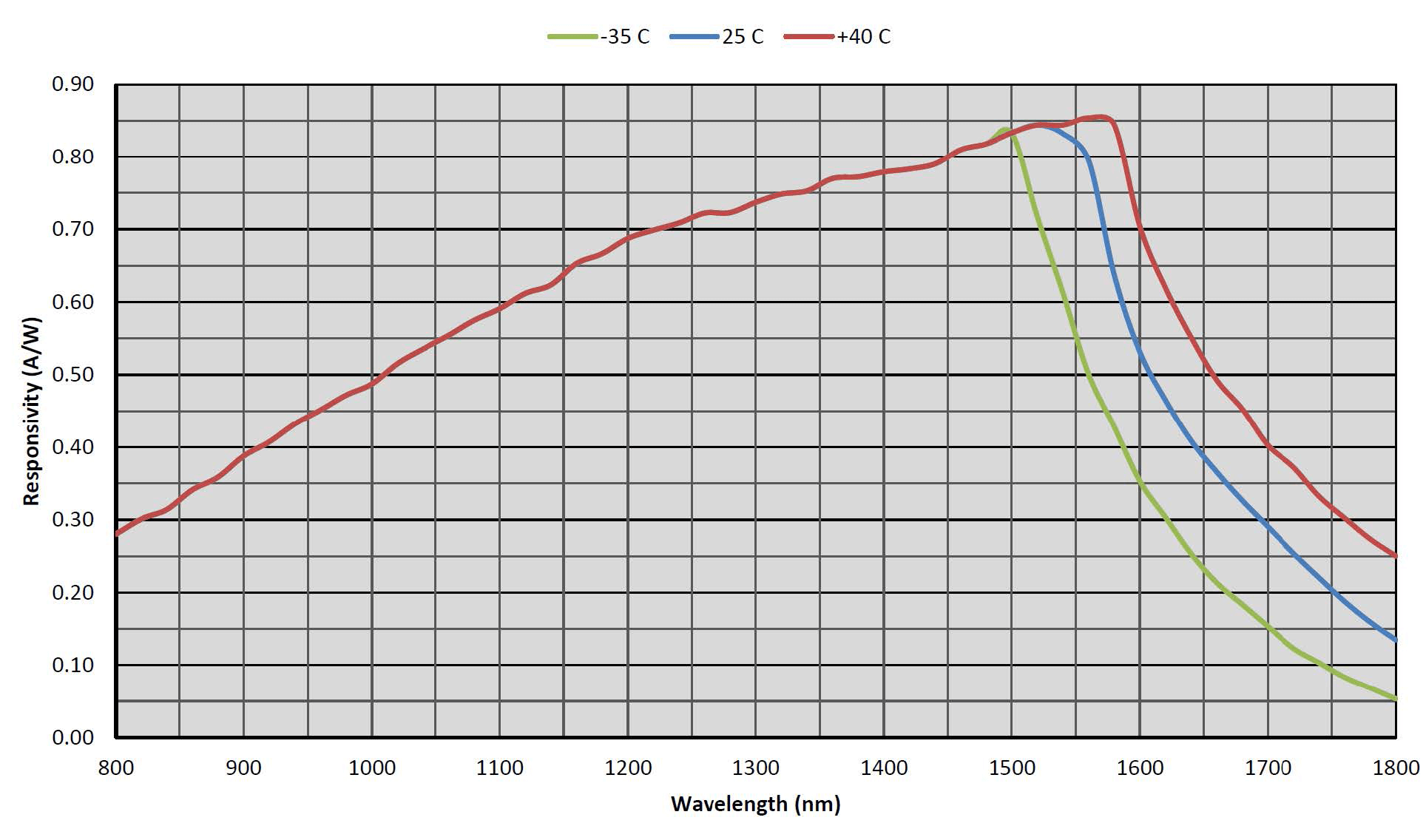
Figure 2-Capacitance vs. Reverse Bias
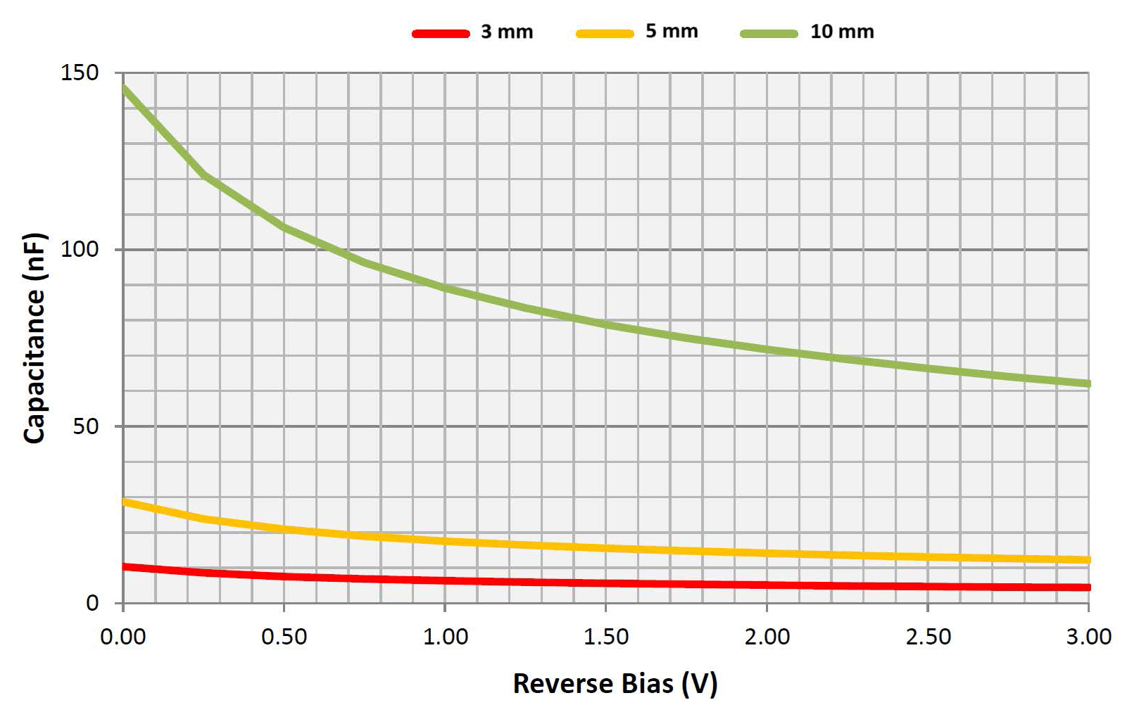
Figure 3-Dark Current vs. Reverse Bias
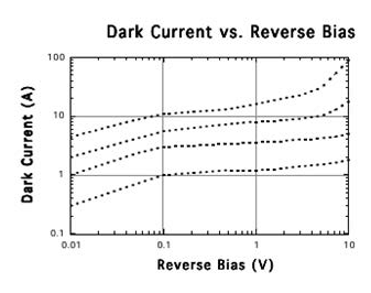
Figure 4-Shunt Resistance vs. Temperature
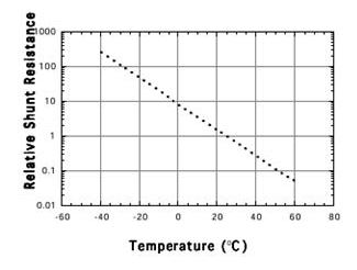
Figure 5. Photocurrent vs. Input Power
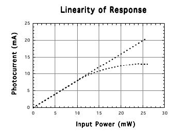
Figure 4-Shunt Resistance vs. Temperature
Figure 5. Photocurrent vs. Input Power


")

")

